Extraction: Devices
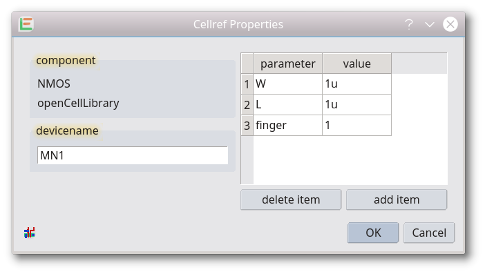
The LayoutEditor can be used to generate a netlist from a layout. To do so any device part of the layout has to be detected and its connection calculated. The device detection is straight forward if the schematic driven layout part of the LayoutEditor is used. In this case, all device information is stored in the layout as properties of the cell reference to the cell representing the device. This information can be viewed with the PropertiesMode by pressing the little component symbol. The symbol is only be visible if the device information is present.
If a device is modified after the schematic driven layout or the layout is done by another software or by parasitic devices, the required information to generate a netlist will not be correct/missing. In that case the device has to be extracted from the layout in a different way. The LayoutEditor includes methods to do so. The required method for each component is described with each component. Check/change it with the EditComponent. The extraction itself is done using ExtractComponent. Alternatively, manual extraction can be performed by ExtractComponent(manual). In both ways new cells will be refered in the layout containing all required device information. With DeleteExtractedDevices previously extracted devices are removed from the layout. These automatic extraction methods are available:
C-parallelPlate
Parallel plate capacitors are detected and calculated. The capacitance area is the overlap of layerA and layerB.
| Extraction Method Parameter | |
|---|---|
| layerA | capacitors electrode layer 1 |
| layerB | capacitors electrode layer 2 |
| areaCap | area capacitance in F/m² |
| edgeCap | edge capacitance in F/m |
| layerContactA | connection layer for electrode 1, used for connector placement (optional) |
| layerContactB | connection layer for electrode 2, used for connector placement (optional) |
| layerPlaceA | layer used for connector 1 (optional) |
| layerPlaceB | layer used for connector 2 (optional) |
| ports | comma separated list of ports as used by the component, order: top, bottom |
| Device Parameter Values | |
|---|---|
| $capSci | capacitance in scientific notation (e.g. 1.4e-5) |
| $capEng | capacitance in engineering notation (e.g. 140n) |
C-nodeToGround
Calculates the capacitance of all shapes of an node to ground. Node of refered cell references without a connection to the current call are not calculated. However any shape connected to the current cell is considered. Shapes on layers not listed with area and edge caps are not considered.
| Extraction Method Parameter | |
|---|---|
| areaCap[layerName1] | area capacitance in F/m² |
| edgeCap[layerName1] | edge capacitance in F/m |
| areaCap[layerName2] | area capacitance in F/m² |
| edgeCap[layerName2] | edge capacitance in F/m |
| ... | |
| ports | port as used by the component |
| Device Parameter Values | |
|---|---|
| $capSci | capacitance in scientific notation (e.g. 1.4e-5) |
| $capEng | capacitance in engineering notation (e.g. 140n) |
MOS-default
A typical 3 connector MOS transitor, optional layerRequiredWell and layerOutsideWell can be used to separate between NMOS and PMOS.
| Extraction Method Parameter | |
|---|---|
| layerPoly | poly layer |
| layerActive | active layer |
| layerContact | contact layer |
| layerRequiredWell | layer of a optional required well |
| layerOutsideWell | layer of a well not covered by the component |
| ports | comma separated list of ports as used by the component, order:source,drain,gate |
| Device Parameter Values | |
|---|---|
| $lengthSci | transitor length in scientific notation (e.g. 1.4e-5) |
| $lengthEng | transitor length in engineering notation (e.g. 140n) |
| $widthSci | transitor length in scientific notation (e.g. 1.4e-5) |
| $widthEng | transitor length in engineering notation (e.g. 140n) |
| $areaSourceSci | area of source contact in scientific notation |
| $areaSourceEng | area of source contact in engineering notation |
| $perimeterSourceSci | perimeter of source contact in scientific notation |
| $perimeterSourceEng | perimeter of source contact in engineering notation |
| $areaDrainSci | area of drain contact in scientific notation |
| $areaDrainEng | area of drain contact in engineering notation |
| $perimeterDrainSci | perimeter of drain contact in scientific notation |
| $perimeterDrainEng | perimeter of drain contact in engineering notation |
BJT-vertical
Detects and extracts a typical vertical bipolar junction transistor.
| Extraction Method Parameter | |
|---|---|
| layerBurried | layer of the buried conductor |
| layerContact | contact layer |
| layerDeep | layer of deep diffusion to contact buried layer |
| layerWell | layer of the basic well |
| layerDiffusion | layer of the diffusion of the emitter |
| ports | port as used by the component |
| Device Parameter Values | |
|---|---|
| none |
BJT-lateral
Detects and extracts a (parasitic) lateral bipolar junction transistor.
| Extraction Method Parameter | |
|---|---|
| layerBurried | layer of the buried conductor (basic) |
| layerContact | contact layer |
| layerDeep | layer of deep diffusion to contact buried layer |
| layerWell | layer of the emitter/collector well |
| maximalEmitterDistance | maximal distance of collector and emitter |
| ports | port as used by the component |
| Device Parameter Values | |
|---|---|
| none |
R-thinFilm
Calculates a thin film resistor. Resitive and connecting layers have to be specified. Resistance is calculated with finite differences. 2 connector and 3 connector resistors are supported. Where there are resistors with more connectors, the resulting resistance between all connectors is extracted. Multi connections per connector are detected and fully supported.
| Extraction Method Parameter | |
|---|---|
| layerResistance | resistive layer |
| layerContact | connecting layer |
| rsquare | square resistance of the resistive layer |
| resolution | resolution of the finite differences calculation. Values between 0 and 100 |
| ports | port as used by the component |
| Device Parameter Values | |
|---|---|
| $resSci | resistance in scientific notation (e.g. 1.4e-5) |
| $resEng | resistance in engineering notation (e.g. 140n) |
© 2026 juspertor GmbH