Technology Tools
The LayoutEditor includes some technology-specific tools. These tools are located at Mainmenu/Utilities/Technology. Most of the tools are Macros and can be adjusted by the user for their used technology.
Printed Circuit Borads (PCB)
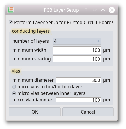
Layer setup for PCB
A layer setup for Printed Circuit Boards (PCB) is performed and a common parameter for the technology layers can be set. Some PCB specific features and PCB file formats like Eagle of KiCad, require a special setup of layers. Predefined layer numbers must be used for conductive layers. This feature will setup typical parameters for PCBs. A fine adjustment can be made afterward in the LayerManager. The PCB place option will also be activated by this feature.
Placement Side Change for PCB
The placement side of PCB components will be changed for all selected component/cell references. The layers in the referred cell will be mapped. A layer setup for Printed Circuit Boards (PCB) is assumed. Such a setup can be made with PCBLayerSetup. This feature is also available in the context menu of the place mode and SelectEditMode if the PCB place option is active.
Copper Fill for PCB
Fills empty space in a PCB conductor layer. Space to conductors as well as the minimum size of created polygons can be set.
OpenCellLibrary
The OpenCellLibrary is a physical design kit (PDK) for an Integrated Circuit design with the LayoutEditor. It is not checked in real IC fabrication and only intended for educational and demonstration use. Technology setup and standard cells are based in the OpenCellLibrary published by Nangate. It was modified for adaption into the LayoutEditor to make it more realistic. To make it a complete PDK for the LayoutEditor, and a template for any further LayoutEditor PDK, it is extended to include parametric cells, symbols, design rule check macros, etc.. Please also read Nangates copyright on the library before using it outside any educational purpose.
© 2026 juspertor GmbH